


根据Verilog代码画电路图
作者:XYZ
本文为明德扬原创文章,转载请注明出处!
FPGA的设计本质是硬件设计,而Verilog是用来描述电路的,所以在学习FPGA的过程中,我们要学会建立电路和Verilog的对应关系,学会看到电路图,就能写出相应的Verilog代码;看到Verilog代码,就能画出相应的电路图。
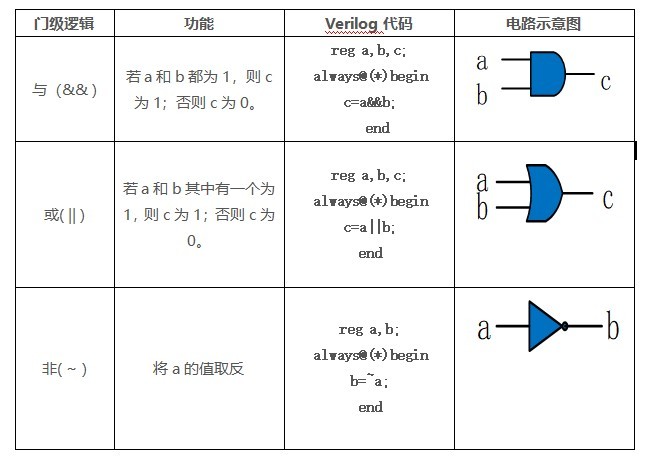
一、门及逻辑
FPGA中常用到的门级逻辑有“与门”、“或门”、“反相器(非门)”等。
以下是1位逻辑“与(&& )”、“或( || )”、“非( ~ )”的功能和Verilog代码及其电路示意图:
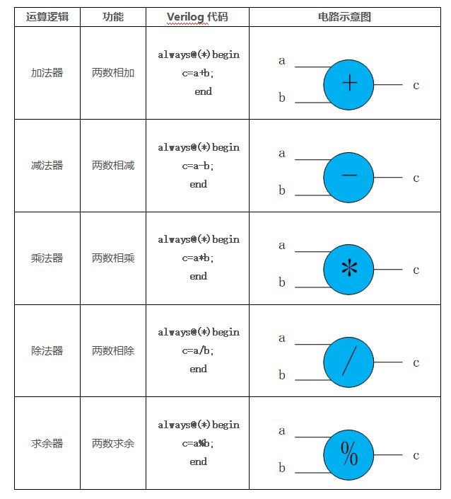
二、运算逻辑
FPGA中常用到的运算逻辑有“加法器”、“减法器”、“乘法器”、“除法器”、“求余器”等。
以下是“加法器”、“减法器”、“乘法器”、“除法器”、“求余器”的功能和Verilog代码及其电路示意图:
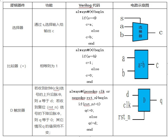
四、根据代码画原理图
FPGA中常用到的逻辑器件有“选择器”、“比较器”、“D触发器”等。
以下是“选择器”、“比较器(下面只对等于(=)比较器进行介绍)”、“D触发器(下面只对FPGA中常用到的D触发器形式进行介绍)”的功能和Verilog代码及其电路示意图:
下图是一段Verilog的代码以及对其的分析并画电路图:
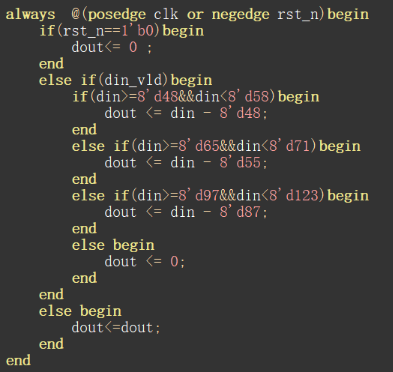
(一)D触发器
该代码中用到一个D触发器的Verilog代码形式,故需要用到一个D触发器:
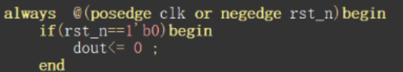

(二)选择器
该代码中用到了四个条件判断语句(if(),else if()形式)的选择器的Verilog代码形式,故需要用到四个选择器:
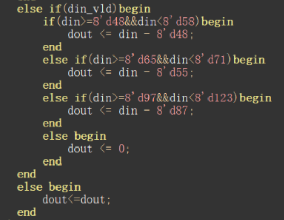

从代码中可以看出:
第一个选择器的选择条件s是din_vld,满足选择条件的选择值a等于以下三个选择器的最终输出值,另一个不满足选择条件的选择值b等于输出值c的反馈值(即保持输出值不变),故第一个选择器的电路图如下:

第二个选择器的选择条件s是din>=8’d48&&din<8’d58(该形式是比较器和与门合成的形式),满足选择条件的选择值a等于din-4’d48(该形式是减法器的形式),另一个不满足选择条件的选择值b等于第三个选择器的输出值或者第四个选择器的输出值或者等于0,故第二个选择器的电路图如下:

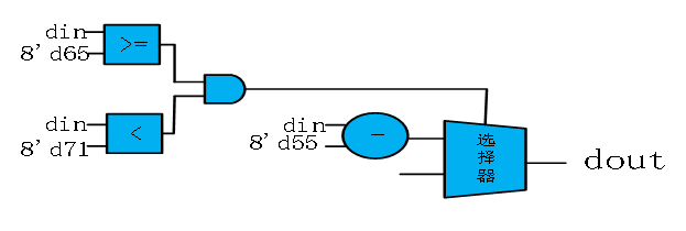
第三个选择器的选择条件s是din>=8’d65&&din<8’d71(该形式又是比较器和与门合成的形式),满足选择条件的选择值a等于din-8’d55(该形式是减法器的形式),另一个不满足选择条件的选择值b等于第四个选择器的输出值或者等于0,故第三个选择器的电路图如下:
第四个选择器的选择条件s是din>=8’d97&&din<8’d123(该形式又是比较器和与门合成的形式),满足选择条件的选择值a等于din-8’d87(该形式是减法器的形式),另一个不满足选择条件的选择值b等于0,故第四个选择器的电路图如下:

综上所述,可以将第四个选择器的输出端连接到第三个选择器的选择值b端,将第三个选择器的输出端连接到第二个选择器的选择值b端,将第二个选择器的输出端连接到第一个选择器的选择值a端。因此最终该Verilog代码的电路图可画成如下所示: