


明德扬专注于FPGA培训:设有 FPGA网络班、FPGA就业班
什么时候SPI
SPI是一个简单的接口,允许一个芯片与一个或多个其他芯片通信。
让我们从一个简单的例子开始,其中只有两个芯片必须通信在一起。
SPI需要在两片芯片之间使用4根线。
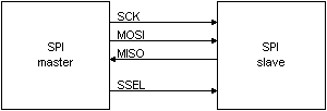
正如您所看到的,这些线被称为SCK、MOSI、MISO和Ssel,其中一个芯片被称为SPI主芯片,而另一个芯片称为SPI从机。
SPI基础
基本上:- 它是同步的。
- 是全双工系列。
- 这不是即插即用。
- 有一个(而且只有一个)主人和一个(或更多)奴隶。
- 同步:时钟由主程序产生。
- 全双工串行:数据被串行化,在每个时钟周期内每个方向传输一位数据,因此使用两条数据线(MOSI和MISO)。
- 不是即插即用:主从双方事先知道通信的细节(位顺序、交换数据的长度等)。
- 一个主从:从不能发起通信,只有主可以。奴隶倾听并回应。
简单转移
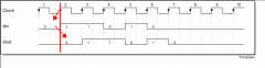
让我们假设主从期望8位数据传输,首先传输MSB。
下面是一个8位数据传输的外观。
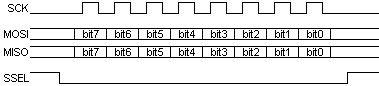
MOSI行是“主输出”,MISO是“从输出”。由于SPI是全双工,两行同时切换,不同的数据从主从和从到主。
详情如下:
- 主从将ssel拉下来,以指示通信正在启动(ssel处于低活动状态)。
- 主开关时钟8次,并在其MOSI线路上发送8位数据。同时,它从MISO线路上的从站接收8个数据位。
- 主人拉起ssel表示转移已经结束。
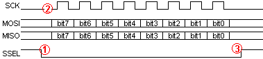
如果主机有多个8位数据要发送/接收,则只有在完成时才能继续发送/接收和取消断言。
多个从机
SPI主机可以通过两种方式与多路从站进行通信:通过并联连接大多数信号并添加ssel线,或者通过将从机链接起来。

使用多条流线技术,一次只能激活一条流线,而未被选择的从线不能驱动MISO线。
简单实现
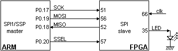
ARM处理器
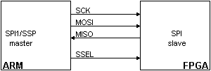
为了有机会测试我们新获得的SPI知识,我们使用萨克索-L董事会。它有ARM 7处理器(LPC 2138)和旋风FPGA(EP1C3),通过SPI总线连接。
ARM用作SPI主电路,FPGA作为SPI从机。Saxo-L ARM处理器实际上有两个SPI接口,一个称为SPI 0,另一个称为SPI 1/SSP。它们都同样容易使用。我们在Saxo-L上使用SPI 1/SSP,因为它是预先连接在板上的。
SPI主C ARM代码
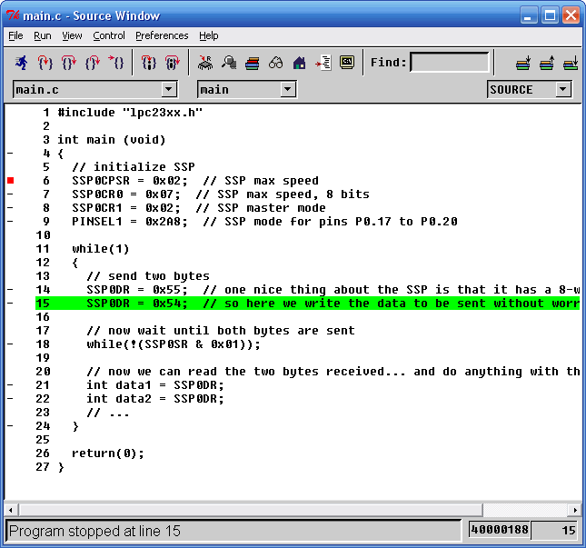
使用SSP只是初始化几个寄存器,然后写入/读取数据以自动发送/接收。.
void main(void) { // initialize SSP SSP0CPSR = 0x02; // SSP max speed SSP0CR0 = 0x07; // SSP max speed, 8 bits SSP0CR1 = 0x02; // SSP master mode PINSEL1 = 0x2A8; // SSP mode for pins P0.17 to P0.20 while(1) { // send two bytes SSP0DR = 0x55; // one nice thing about the SSP is that it has a 8-words deep FIFO SSP0DR = 0x54; // so here we write the data to be sent without worrying // now wait until both bytes are sent while(!(SSP0SR & 0x01)); // now we can read the two bytes received... and do anything with them int data1 = SSP0DR; int data2 = SSP0DR; // ... } }SPI从HDL FPGA码
现在用于FPGA中的SPI从站。
由于SPI总线通常比FPGA工作时钟慢得多,所以我们选择使用FPGA时钟对SPI总线进行过采样。这使得从代码稍微复杂一些,但它的优点是在FPGA时钟域中运行SPI逻辑,这将使以后的工作变得更容易。
首先是模块声明。
moduleSPI_slave(clk, SCK, MOSI, MISO, SSEL, LED);inputclk;inputSCK, SSEL, MOSI;outputMISO;outputLED;请注意,我们有“CLK”(FPGA时钟)和一个LED输出。一个不错的调试工具。“CLK”需要比SPI总线更快。Saxo-L的默认时钟为24 MHz,在这里工作得很好。
我们使用FPGA时钟和移位寄存器对SPI信号(SCK、SSEL和MOSI)进行采样/同步。
// sync SCK to the FPGA clock using a 3-bits shift registerreg[2:0] SCKr;always@(posedgeclk) SCKr <= {SCKr[1:0], SCK};wireSCK_risingedge = (SCKr[2:1]==2'b01); // now we can detect SCK rising edgeswireSCK_fallingedge = (SCKr[2:1]==2'b10); // and falling edges // same thing for SSELreg[2:0] SSELr;always@(posedgeclk) SSELr <= {SSELr[1:0], SSEL};wireSSEL_active = ~SSELr[1]; // SSEL is active lowwireSSEL_startmessage = (SSELr[2:1]==2'b10); // message starts at falling edgewireSSEL_endmessage = (SSELr[2:1]==2'b01); // message stops at rising edge // and for MOSIreg[1:0] MOSIr;always@(posedgeclk) MOSIr <= {MOSIr[0], MOSI};wireMOSI_data = MOSIr[1];现在从SPI总线接收数据很容易。
// we handle SPI in 8-bits format, so we need a 3 bits counter to count the bits as they come inreg[2:0] bitcnt;regbyte_received; // high when a byte has been receivedreg[7:0] byte_data_received;always@(posedgeclk)beginif(~SSEL_active) bitcnt <= 3'b000;elseif(SCK_risingedge)beginbitcnt <= bitcnt + 3'b001; // implement a shift-left register (since we receive the data MSB first) byte_data_received <= {byte_data_received[6:0], MOSI_data};endendalways@(posedgeclk) byte_received <= SSEL_active && SCK_risingedge && (bitcnt==3'b111); // we use the LSB of the data received to control an LEDregLED;always@(posedgeclk)if(byte_received) LED <= byte_data_received[0];最后是传输部分。
reg[7:0] byte_data_sent;reg[7:0] cnt;always@(posedgeclk)if(SSEL_startmessage) cnt<=cnt+8'h1; // count the messagesalways@(posedgeclk)if(SSEL_active)beginif(SSEL_startmessage) byte_data_sent <= cnt; // first byte sent in a message is the message countelseif(SCK_fallingedge)beginif(bitcnt==3'b000) byte_data_sent <= 8'h00; // after that, we send 0selsebyte_data_sent <= {byte_data_sent[6:0], 1'b0};endendassignMISO = byte_data_sent[7]; // send MSB first // we assume that there is only one slave on the SPI bus // so we don't bother with a tri-state buffer for MISO // otherwise we would need to tri-state MISO when SSEL is inactiveendmodule我们已经建立了ARM和FPGA之间的通信!
运行代码
当我们通过ARM代码时,我们可以看到LED的变化状态,以及FPGA返回的数据。